Lab 1: FPGA and MCU Setup and Testing
Hours spent on lab: 12 Hours
Overview
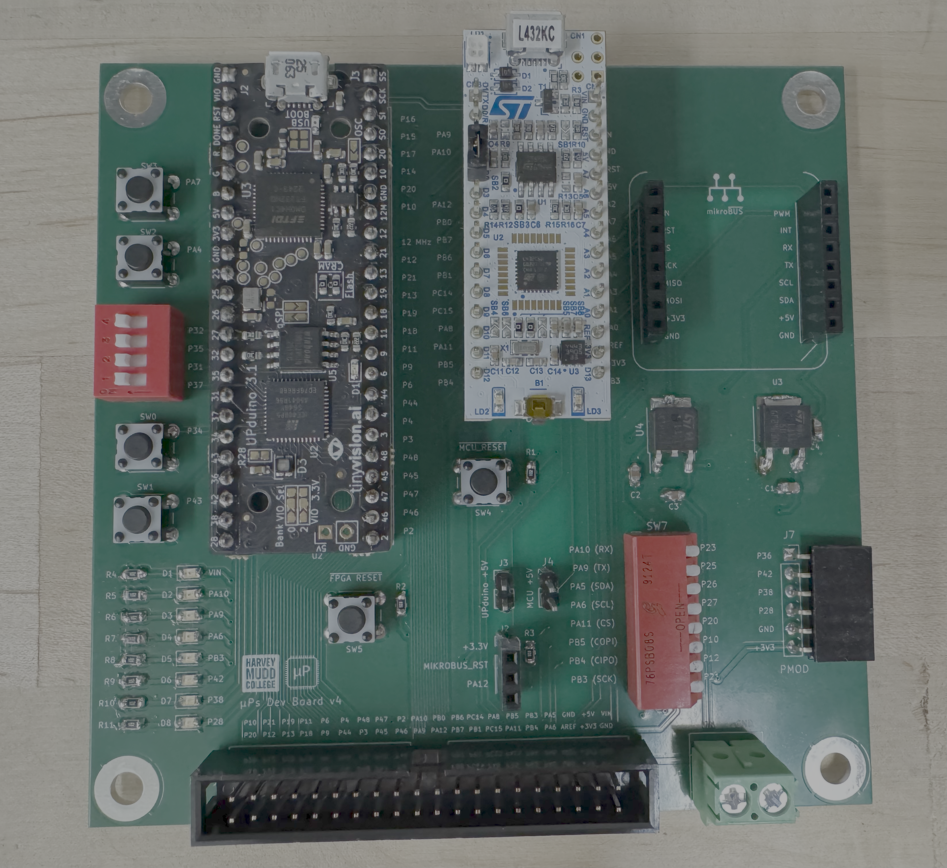
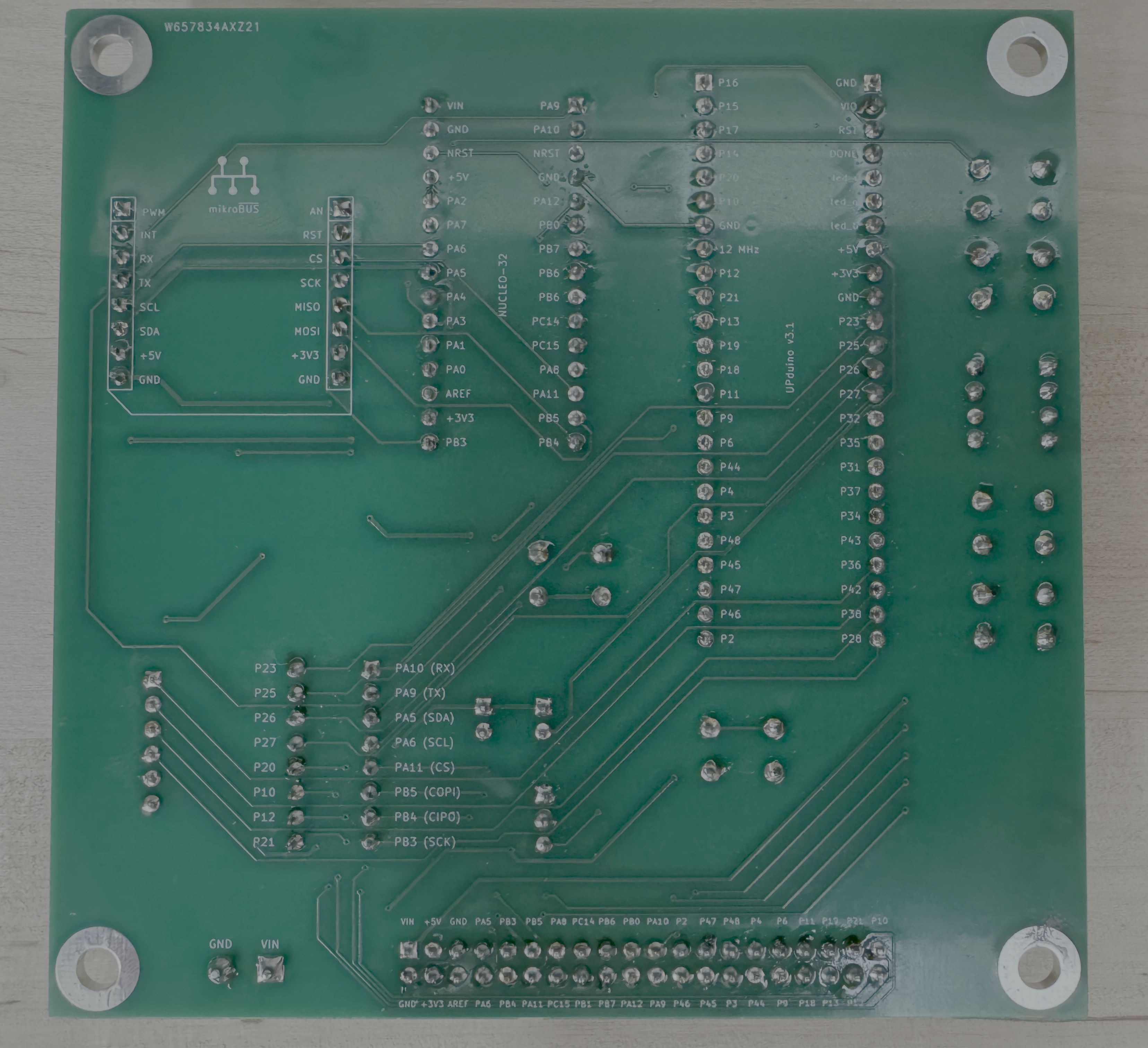
In this lab, the microcontroller and FPGA development board we will use for the continuation of this semester of E155 was soldered and assembled. We verified it was working correctly by uploading some demo code to make an onboard LED blink at \(1\) Hz.
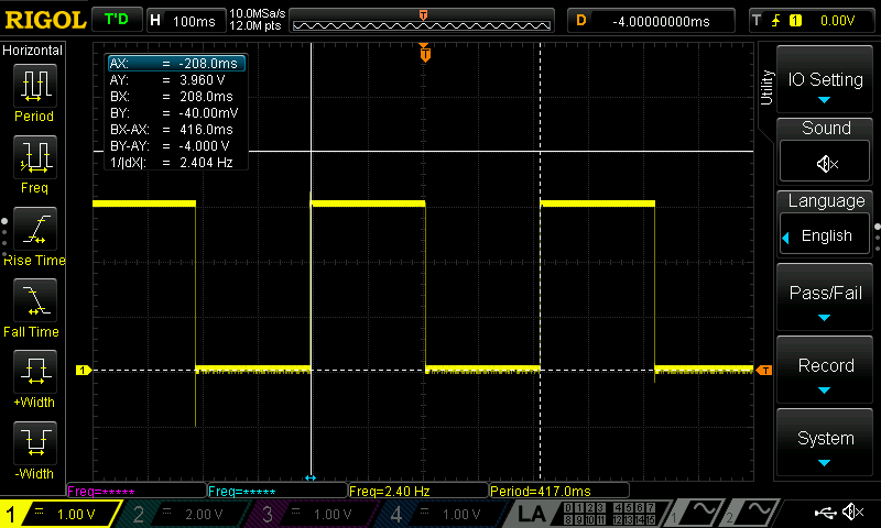
The rest of the lab consisted of making some combinational logic to turn on onboard LEDs in addition to making another onboard LED blink at \(2.4\) Hz and more combinational logic to display a digit in a 7-Segment-Display depending on the binary input. This is shown below.
| Input | Output | Logic |
|---|---|---|
| S[0:1] | Onboard Led 0 | XOR |
| S[2:3] | Onboard Led 1 | AND |
| \(48\) Mhz Oscillator | Onboard Led 2 | 2.4 Hz Blinking |
| S[0:6] | 7 Segment Display | Binary Decoder |
Hardware Setup
I followed the Lab 1 guide for assembling and soldering my development board in addition to the interactive site.
Calculations
Assuming our 7 Segment Display LEDs have a drop of 2V and we want to restrict the current flow through the display to less than 20 milliamps. Using Ohm’s Law: \(V = IR\) we can rearrange to solve for resistance: \(R = \frac{V}{I}\). Then plugging in our values: \(\frac{[3.3 V - 2 V] - 0 V}{20 \times 10^{\3} A} = 65 \Omega\). So I will use a resistor larger than \(65 \Omega\), the nearest size up stocked in the Engineering Stockroom being \(68 \Omega\), restricting the current through the display to \(19\) mA of current.
Methods
I broke up the required tasks into different Verilog modules. In the following block diagram you can see each of my modules and how they fit together.
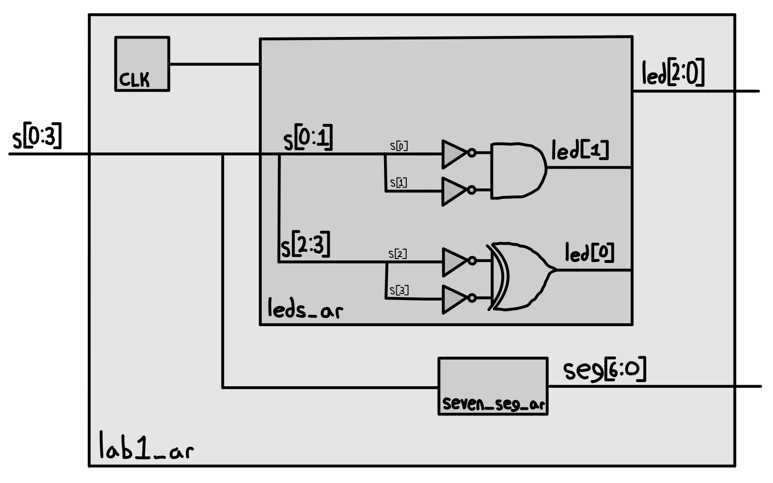
The modules can be found here in my github.
Schematic
The schematic for the circuit includes the FPGA, DIP switches, LEDs, and 7-segment display.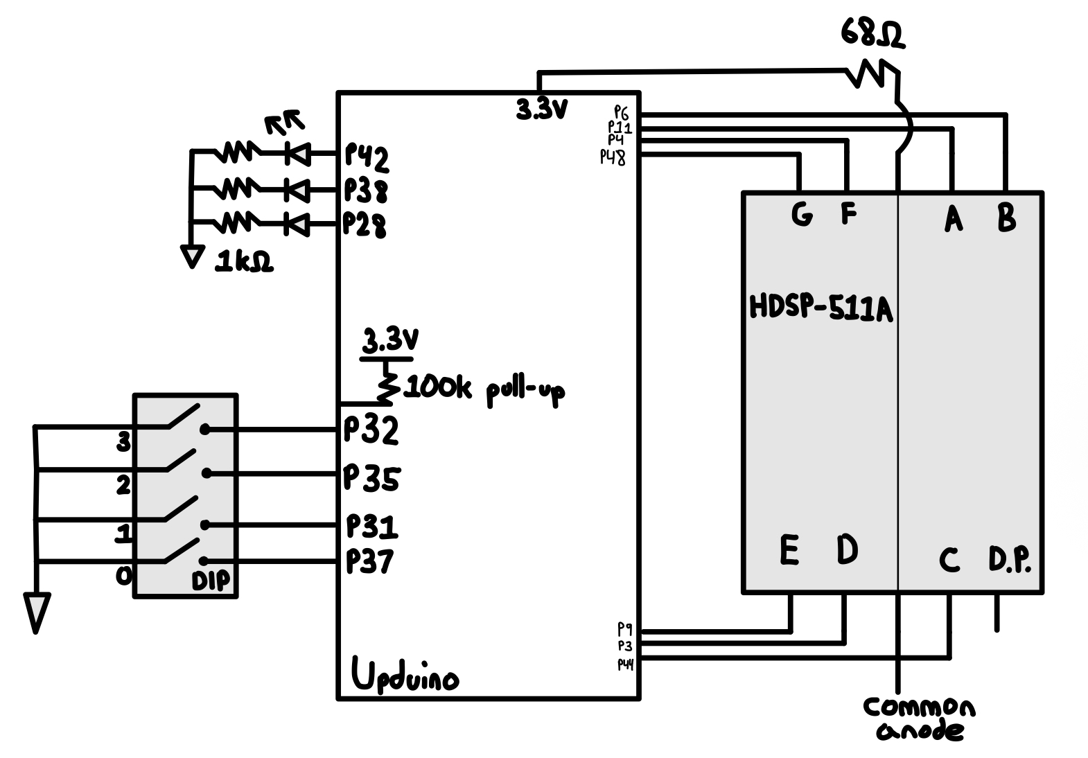
Simulations
I created a testbench for each of the modules I made. The testbenches loads testvectors that simulate all of the combinational logic of switches and LED and 7 Segment Display outputs against each other to make sure the outputs are what I expect when the module is run. You can see below my waveforms generated from my 3 simulations
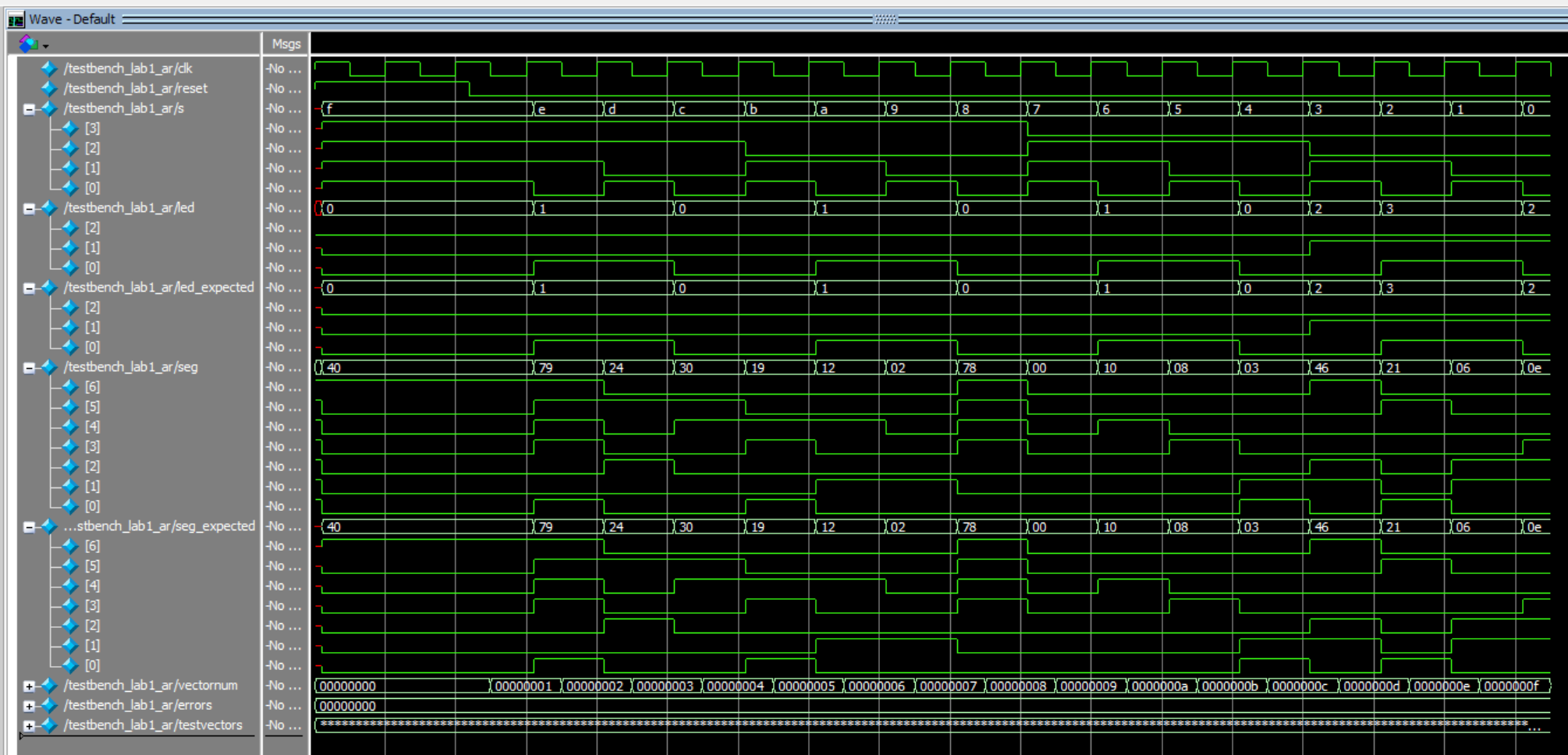
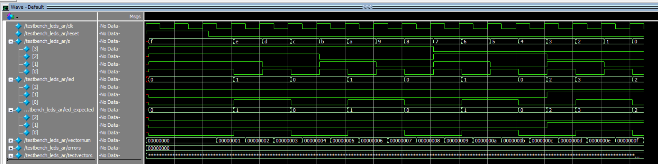
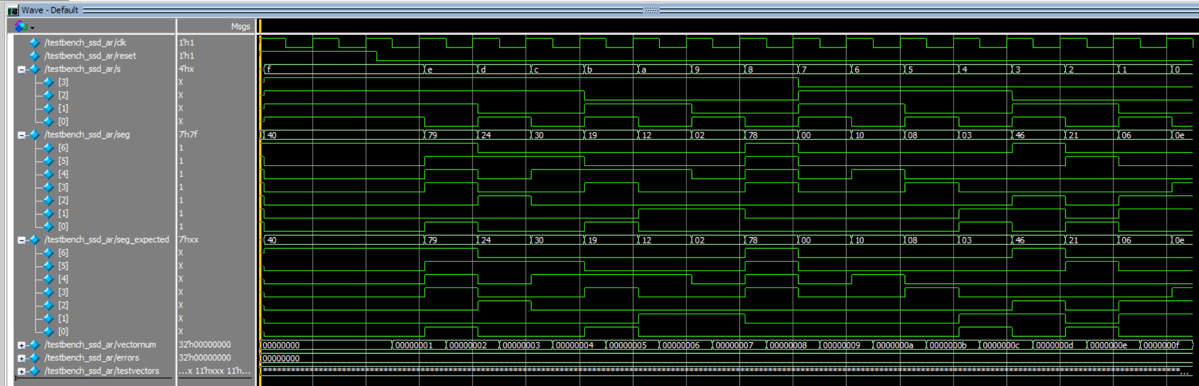
The top level module ran 16 tests with 0 errors !
Hardware Testing
AI Prototype
I used Gemini’s 2.5-Pro model for this section of the assignment.
I prompted the AI with: “Write SystemVerilog HDL to leverage the internal high speed oscillator in the Lattice UP5K FPGA and blink an LED at 2 Hz. Take full advantage of SystemVerilog syntax, for example, using logic instead of wire and reg.”.
Compiling the given code resulted in 1 error and 12 warnings: Error 35901063 Synthesis ERROR <35901063> - c:/users/abrah/onedrive/documents/lab1_ai/source/impl_1/lab1_ai.sv(21): instantiating unknown module SB_HFOSC. VERI-1063 [lab1_ai.sv:21]
It simply suggested I didn’t have the module installed but it was trying to access a oscillator not compatible with our board. I fixed the oscillator declaration for it then it compiled fine.
Results
All lab requirements were met. The E155 development board is fully assembled and operational, except for a broken ribbon cable connector that needs replacement. The FPGA is programmed with synthesized Verilog, successfully driving the LEDs and 7-segment display as specified. Both simulation and hardware tests confirm correct operation, with the 7-segment display showing all digits clearly and equally bright.