Lab 2: Multiplexed 7-Segment Display
Hours spent on lab: 15 Hours
Hours procrastinated: 45 Hours :(
Overview
In this lab, expanding on our 7-segment-display knowledge from Lab 1, we controlled a two digit 7-segment-display with the same pins via multiplexing the power pins based on the clock signal. Controlling each segment with independent combinational logic, we toggle between them fast enough to appear as if they are both independently running. Finally, we display the sum of the two numbers displayed on the digits as a binary sum in the form of LEDs.
Hardware Setup
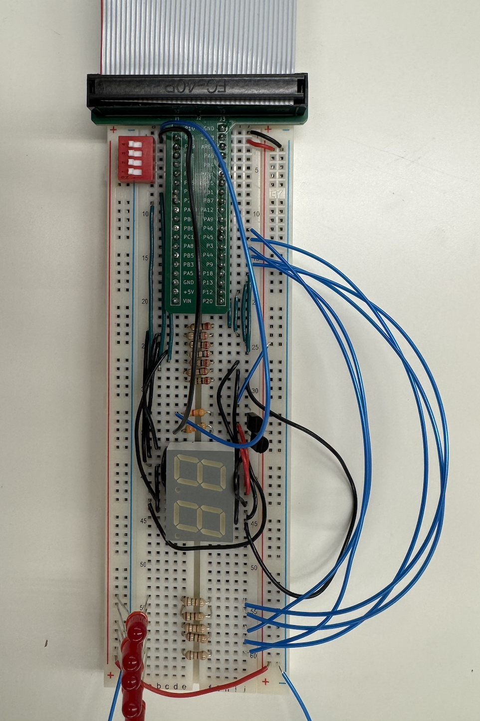
Our FPGA has 18 GPIO pins available for use. The two 7-segment-displays require 7 pins for each segment, and 2 pins for powering them (while an inverter chip could’ve been used, it would’ve been more to breadboard and the pin was available for use). 4 Input pins for the DiP switches and 5 output pins for the summation LEDs, so we utilized all available programmable pins on our FPGA. This is my breadboard:
Calculations
Transistor Current through the Base:
The drop of the diode in the transistor is \(V_{BE} = 700 mV\). Due to this drop, the Base is at \(2.6 V\) and the collector is at \(3.3 V - 250 mV = 3.05 V\). If our red 7-Segment-Display Diodes have a drop of \(1.8V\) … and a safe current into our FPGA is around \(5 mA\) so we can also see our diode light up. \(\frac{3.05 - 0}{5 * 10^{-3}} = 610 \Omega\). So for our power driving resistors … we can safely use a \(610 \Omega\) Resistor or larger.
Driving single LEDs
Since our single red LEDs have a drop of about \(1.8 V\), \(\frac{3.3 V - 1.8 V}{10*10^{-3} A} = 100 \Omega\).
Driving 7-Segment-Display
Since our 7-Segment-Display red LEDs have a drop of about \(1.8 V\), \(\frac{3.1 V - 1.8 V}{5*10^{-3} A} = 260 \Omega\). (From \(3.1 V\) due to Transistor Collector).
Methods
I broke up the required tasks into different Verilog modules. In the following block diagram you can see each of my modules and how they fit together.
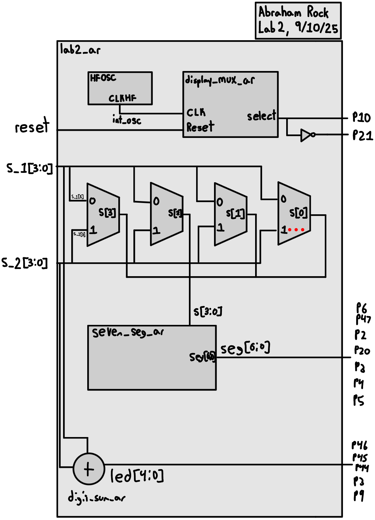
The modules can be found here in my github.
Schematic
The schematic for the circuit includes the FPGA, DIP switches, LEDs, and 7-segment display.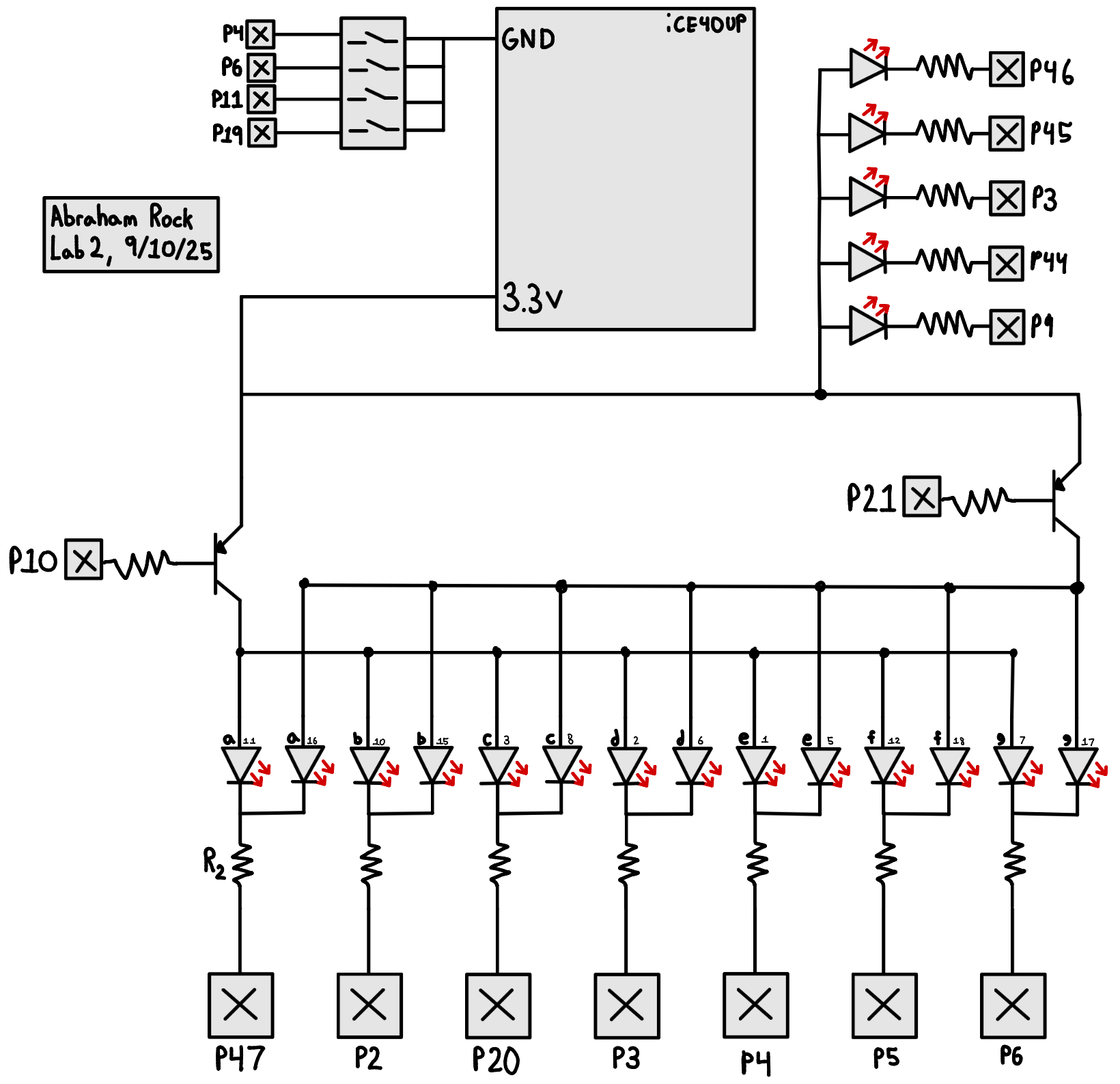
Simulations
AI Prototype
I used Gemini’s 2.5-Pro model for this section of the assignment.
I prompted the AI with: “Write SystemVerilog HDL to time multiplex a single seven segment decoder (that decodes from four bits to a common anode seven segment display) to decode two sets of input bits and drive two sets of seven output bits.”.
The AI-generated code was similar to my approach, splitting the design into a top-level module, a seven-segment decoder, and a multiplexing controller. It also instantiated a high-speed oscillator for timing, which I had to fix in my own implementation due to synthesis errors. The AI’s code provided a good reference for structuring the multiplexing clock logic and handling two sets of input bits. I can appreciate how it does everything in hex too to make things a bit more readable.
For the next prompt: “Write SystemVerilog HDL to time multiplex a single seven segment decoder (that decodes from four bits to a common anode seven segment display) to decode two sets of input bits and drive two sets of seven output bits. Use the seven segment decoder and oscillator provided in the attached files.” It again did a good job that compiled and the logic looked like it would perform well upon upload.
Results
All lab requirements were met. Human eye cannot tell the flickering of my multiplexing at 60Hz. All combinations work with little to no bleed of lights or colors.